Integrated DC/DC converter design for smart card power supply
For the smart card power supply, this paper proposes an integrated DC/DC converter structure and analyzes its working principle. The system is 85% efficient, robust enough to meet all complex ISO7816-3 specifications, and has passed Level 1 and Level 2 certifications for EMV and EMV Co certification procedures. This structure is especially suitable for smart card applications such as portable cash registers (POS).
The operating voltage of the smart card has been upgraded to fit any chip specifically for this application. The original ISO7816-3 and EMV (Europay/Master card/Visa) files now include 1.8V, 3.0V and 5.0V as suitable operating power supplies. Therefore, the physical interface between the card and the microcontroller must be able to adapt any of the above power supplies to the primary MPU. The power supply must maintain the operating conditions specified in Table 1. In addition, the power supply must be able to disconnect the card within 750μs, especially when the card is removed.

In addition to quiescent operation, the power supply keeps the output voltage within tolerance when the load is 100mA/400ns pulsed. Such requirements relate to the state of the system, not just the power source.
DC/DC converter
As applications become more widespread, from battery-powered portable systems to television satellite receivers, smart card interfaces must efficiently handle large input voltage ranges with high efficiency. Basically, it can be implemented in any type of structure as long as it provides the required power to the card. It can be designed as a converter based on switched capacitors, but its limited efficiency becomes a key issue when considering portable POS systems. This is different for GSM applications because the output power is limited to 50mW, so this capacitor-based structure is prioritized on the radiotelephone PCB to save space.
Considering that for POS portable modules, energy savings are a key issue, so inductor-based structures are prioritized to maximize efficiency. In fact, with an output power of up to 300mW, the efficiency of the inductor structure can reach 85% over the entire operating voltage range, which is difficult to achieve with low-cost switched capacitor technology.
On the other hand, because the input voltage can range from a minimum of 2.70V to a maximum of 5.50V (after the battery runs out or after the battery is charged), the structure must be switched from boost to buck, automatically and without adjustment, and vice versa. . The concepts depicted in Figure 1 have been developed to meet these requirements, with EMV certification being the primary goal in design.

Real systems implemented in silicon dies are more complex because they can neither have voltage spikes while performing precise adjustments and low ripple. Most importantly, the circuit must meet all EMV specifications, especially the power down sequence, power down sequence, and output short circuit current.
To meet these requirements, the converter shown in Figure 2 adds several additional NMOS and PMOS transistors.

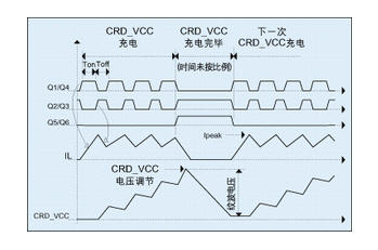
The system operates in a two-cycle concept (see Figure 2 and Figure 3 for all notes) with a special structure that takes into account the requirements of the smart card:
Cycle 1: Q1 and Q4 are turned on, and the inductor L1 is charged by an external battery. At this stage, Q2/Q3 and Q5/Q6 are turned off.
The current flowing through the two MOSFETs Q1 and Q4 is internally monitored and turned off when the Ipeak value (peak current, depending on the programmable output voltage value) is reached. At this point, cycle 1 is complete and cycle 2 begins. The "on" time is a function of the battery voltage and the value of the inductive network (L and Zr) connected between pins 10 and 11.
To prevent uncontrolled operation, the 4μs pause structure ensures that the system operates only in a continuous cycle of 1 cycle with overload or low battery input.
Cycle 2: Q2 and Q3 are turned on, and the energy stored in the inductor L1 is transferred to the external load through Q2. At this stage, Q1/Q4 and Q5/Q6 are turned off. The current flow period is a constant value of 900 ns (typical), and if the CRD_VCC voltage is lower than the specified value, the period 1 is repeated after this period of time.
When the output voltage reaches the specified value (1.80V, 3.0V or 5.0V), Q2 and Q3 are immediately turned off to avoid overvoltage on the output load. At the same time, two additional NMOSs, Q5 and Q6, are turned on to completely drain the current stored in the inductor, avoiding ringing and voltage spikes on the system. Figure 3 shows the theoretical waveform of the DC/DC converter.

When CRD_VCC is programmed to 0V, or when the smart card is removed from the socket, the active pull-down Q7 quickly discharges the output storage capacitor, ensuring that the output voltage is below 0.40V when the card is taxied on the ISO contact. Due to the low on-resistance of Q7, the output voltage drops rapidly to 400mV in less than 100μs, well below the maximum 750μs specified by EMV.
Output voltage ripple, although not directly specified by ISO7816-3 or EMV, plays an important role in the operation of smart cards. Its peak-to-peak value depends on the following two main electrical parameters:
1. The total series resistance between the output silicon structure and the net storage capacitor;
2. Regulation, the ability to detect an output voltage with a minimum threshold and hysteresis.
The first parameter depends on the internal bond wire that the chip is connected to the outside world, the pin contact that connects the series resistor of the storage capacitor, and the printed circuit board copper wire that connects the pin to the load. When a large current is passed through the pin, multiple wire bonding techniques are widely used to reduce the series resistance to 50 m (or a lower resistance value if a wider weld line is used).
The width of the printed circuit board traces can be tailored to the current processing needs of a given application. In addition, this series resistance can be a problem as the external passive components involved vary widely from application to application. The most critical part is the storage capacitor, because (for economic reasons) the low-cost type is generally preferred, but this creates a high-voltage spike that is almost impossible to completely eliminate.
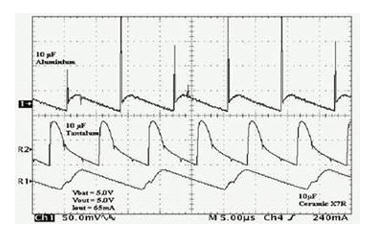
Depending on the type of technology used to develop the capacitor, the parasitic element may have a relatively high value, resulting in a large uncontrollable spike. As shown in Figure 4, this equivalent series resistance (ESR) is very susceptible to such spikes because the supply current flows directly through it and brings high voltage pulses into the output source.

Based on experiments conducted in the NCN6001 and NCN6004A characterization, the best solution is to use two parallel 4.7μF/10V/ceramic/X7R capacitors to achieve CRD_VCC filtering. The ESR does not exceed 50m over the entire temperature range, and the combination of standard components provides an acceptable tolerance of -20% to +20% with limited cost increases. Table 2 gives a rough comparison of the most common types of capacitors. Figure 5 shows the CRD_VCC ripple observed on the NCN6001 or NCN6004A demo board for different capacitor types for output voltage filtering. The large and fast transients observed on the above curves are very difficult to filter because of their high energy. It is clear that aluminum capacitors are not suitable for this type of application and should be avoided.

The second parameter depends on the performance of the internal comparator, voltage reference tolerance, and digital processing. The voltage reference is derived from a precisely stable bandgap circuit, resulting in a tolerance of ±3%. On the other hand, the deviation and drift of the analog function is reduced by high-end integration techniques. A detailed analysis of DC/DC operation helps to understand the effect of each component on the output voltage ripple (see Figure 2 and Figure 6).
In operation, the inductor current alternates between the Iv and Ip values, as shown in Figure 6. When the system changes from cycle #1 to cycle #2, the energy accumulated in the inductor is transferred to the load, and the storage capacitor voltage increases as energy transfers to it.

Let k = R1/(R1 + R2). When Vo is greater than k*Vref, the internal comparator U1 flips and the output current drops to zero at time t1. Correspondingly, the output capacitor carries all of the energy previously stored in the inductor, and the output voltage remains above the reference value specified by the parameter k*Vref. The final voltage Vohp represents the high-end ripple amplitude.

At this point, the output voltage begins to drop (because there is no more energy in the inductor), and depending on the time t2 determined by the load, the comparator flips when Vo is less than k*Vref. The DC/DC converter continues to cycle #1, but the output voltage continues to drop because more time is required to reach the Ip current value (time t3) and the inductor is charged from zero. Finally, when the low-end Volp of the ripple amplitude is reached, cycle #2 begins a new cycle. The waveform of Figure 6 depicts this mechanism.
Conclusion of this paper
A DC/DC converter with an efficiency of 85% in working conditions has been developed for smart card power supply to meet all complex ISO7816-3 specifications. The system is robust enough to prevent system latching when the load changes rapidly from zero to peak, even when the battery is at either end of the input voltage range. In addition, the short-circuit current protection avoids any thermal runaway because the overload current trigger point decreases as the temperature increases. This architecture has been certified to Level 1 and Level 2 by EMV and EMV Co certification procedures, including the EMV2000 protocol.
Electric Standing Desk Converter
Electric Standing Desk converter is controled by electricity. You can easily to adjust the height to a perfect height for you.
Freely height adjustment -- Once you find your ideal height, our smart height locking mechanism locks the desk in place. You can transform any desk into a comfortable workstation that suitable for your needs at any time. It gets you out of your chair to relieve muscle tension, improve blood circulation, reduce stress, and increase productivity. Desk Converter is a minimalist and an affordable & feasible solution for sitting or standing at work.
Different models of stand up desk converter and monitor riser: Manual, gas lifting and electric Desk Riser , costomize tabletop colors and sizes.
Some hotselling desk adjuster have spacious two-tier desktop: Add up to 2 monitors on the roomy top tier plus a keyboard and mouse or laptop on the lower tier. The ergonomic two-tier design provide you perfectly for ideal studying and working space.
Convenient gas spring lift and single-handle design let you smoothly switch from sitting to standing.This series of desk riser have a sturdy and stable steel frame. Our durable and heavy-duty steel frame provides maximum stability at every level. No matter sitting or standing, you can safely work with confidence.
We have many series of computer standing desks to help point you in the right work direction. Whether you want something that`s high-end and elegant, affordable, high quality or a Gaming Desk , laptop desks, there`s something on our products list to suit your comfort and wellness needs. We offer the best compuer desk, movable laptop table, office chairs, Laptop Desk , Sit Stand Desk, office exercise bike and an under-desk treadmill to make your work experience healthier.
Lifting desk stand, Electric height adjustable standing desk convertor, Adjustable standing desk converter, Desk coverter
Foshan Hollin Furniture Co.,Ltd , https://www.china-hollin.com